Project on Remote Sensing
PRACTICAL TRAINING
AT
DEFENCE LABORATORY, JODHPUR
TOPIC: - Remote Sensing, Digital Image Processing and some electronics instrumentation projects.
CONTENTS
1. INTRODUCTION TO REMOTE SENSING AND DIGITAL IMAGE PROCESSING
2. FUNCTIONAL REQUIREMENTS OF THE SYSTEM
Ø RPM SENSOR
Ø THE 8751 MICROCONYROLLER
3. CIRCUIT DIAGRAMS
4. CIRCUIT DESCRIPTION
5. PROGRAM CODING
6. CONCLUSION
PREFACE
The summer training for IV semester was completed from Defence Laboratory, Jodhpur a Research Laboratory under Ministry of Defence, Defence Research and Development Organization. The work place allotted within the laboratory was Remote Sensing Group. The group is essentially engaged in activities related to Remote Sensing, Digital Image Processing and some electronics instrumentation projects.
INTRODUCTION: The main activity of the group in which I was placed was remote sensing. The Remote sensing data is obtained from various satellites such as Indian Remote Sensing satellites, LANDSAT of USA, SPOT satellite of France, IKONOS of USA etc. This data comes in different resolutions. The data needs lot of processing before it can be used for analysis of ground cover or details of features on ground. Software for processing of satellite data was demonstrated to us along with ways and means of analysis. The group is also engaged in development of instrumentation and our area of specialization being electronics we were given training in electronics.
SCOPE: The training was aimed at imparting understanding of instrument design using intel’s 8751 microcontroller and I was specifically directed to develop a RPM Counter.
LEARNING OBJECTIVES:
SHORT TERM: The short term objective was to develop RPM Counter using intel’s 8751 microcontroller.
LONG TERM: Long term learning objectives were:
Ø To understand the intel’s 8751 microcontroller
Ø To understand itinerary of instrument design
Ø To be able to develop software in assembly language
Ø To learn the concept of microprocessor development system
METHODOLOGY: Initially I was introduced to the subject of microprocessors in general and 8751 in particular through a series of lectures/ discussions. Familiarization with the software and hardware development environment was thereafter completed. The concept of how to proceed with system design was introduced before the final task was assigned. My progress on the task was regularly monitored and problems encountered were sorted out till the completion of task
CONTENTS OF TRAINING: The training consisted of following activities:
Ø Learning Microprocessor hardware and software through lectures/ discussions.
Ø Familiarization with development environment.
Ø Issues of signal compatibility for sensor connectivity.
Ø Working with 7 segment displays and drivers.
Ø Constructing the circuit on general purpose PCBs.
Ø Burning programs in controller and
Ø Testing of the system
ACHIEVEMENTS: The objectives of the training outlined above were achieved. A RPM Counter for the given sensor was constructed and tested. With additions such as calibration etc. it can be a functional unit.
CONCLUSION: The objectives of the training were completely achieved.
REFERENCES:
1. Intel’s Data sheets on 8751 microcontroller.
2. National semiconductor Datasheets
3. Introduction to Microprocessor: Aditya P. Mathur
4. Microprocessor data Hand book BPB Publications
INTRODUCTION TO REMOTE SENSING AND DIGITAL IMAGE PROCESSING
Remote sensing in the present context can be defined as a tool for getting information about the terrestrial objects from a platform placed at sufficiently high altitude. The field of remote sensing came in prominence after 1950. The availability of multiple data acquisition techniques and data analysis systems made this possible. The remote sensing techniques enhance the capability of human observer. The limitation of line of sight, hindrance caused by undulations of terrain, obstruction of view by natural or artificial objects etc. are automatically overcome as the sensor is at a much higher height than most terrestrial objects. This has become possible due to data acquisition in limited and narrow spectral bands, near IR and thermal IR imaging, microwave imaging etc.
Remote sensing of an area requires: 1. A platform, 2. Suitable Sensor, 3. Data collected from the platform, 4. Some ground based information for assisting the process of information extraction and 5. A computer system along with necessary software for data analysis and output generation.
THE PLATFORM
The platforms can be of wide variety. Cherry picker, Balloons, Aircraft, and satellites of commercial and secrete nature are commonly used platforms. The use of Cherry packer and balloons can yield very high-resolution data since the altitude is low in comparison with other platforms. These platforms are however inconvenient to collect data and not suitable in defence applications since placing these in adversaries area is out of question. The Aircraft is a convenient means of data collection. It can yield high-resolution data and can be deployed for reconnaissance flights. Unmanned aircraft can also be used in specific applications. The aircraft however is susceptible to anti-aircraft missiles. Satellites are the most convenient means of data collection. Commercial data products of any location are readily available and the resolution of these data products is day by day increasing to suit military applications. Recently the IKONOS satellite has been announced with 1m resolution. This resolution can enable detection capability to detect even a single tank placed on ground.
THE SENSORS
These may include aerial cameras, aerial scanners, Satellite based imaging scanners etc. The imaging may again be done in any range of electromagnetic spectra e.g. Microwave, Visible, Near IR or Thermal IR. Depending on the altitude of the sensor and the scanner used the resolution of the data changes. The resolution or pixel size is defined as the area represented by a single data point. The spectral specifications include number of bands and the spectral response of each of them. Details on this topic are discussed in the lecture on SENSORS.
The following figure illustrates a typical data acquisition system used in remote sensing. The platform shown is a satellite. The sensor shown is a typical scanning imager. The satellites, which are generally launched in the sun-synchronous orbit, revolve in plane orthogonal to the equatorial plane. The satellite while passing over any locations scans the ground in the different spectral bands. The reflection from the earth surface is digitized and the digital data is transmitted to the data receiving stations.
DIGITAL IMAGE PROCESSING
Processing of any two dimensional data is termed as image processing. Such data may be satellite scanner imageries, X-ray photographs, temperature profiles of an object, CAT scan images, aerial scanner data or any other two dimensional data. This is a wide definition and includes image processing by visual as well as digital means. The part of image processing that shall be discussed in this lecture is digital image processing. Optical image processing tools are also used, which are convenient and fast. The limitation of optical processing is the complexity of the systems and their inability in generation of outputs of statistical and numerical nature. Quantification of parameters using optical processing is difficult.
Digital image processing techniques can be further divided into seven sub-sections. These are, 1. Image representation, 2. Image transforms, 3. Image restoration, 4. Image enhancement, 5. Image reconstruction, 6. Image analysis and 7. Data compression.
The brief summary of each of these processes is discussed here:-
IMAGE REPRESENTATION
A digital image is a set of numbers represented in matrix format. Fig. 1 shows a sample digital image. The image data placed in such format or any other suitable format is termed as image representation
|
|
a2,1 |
... |
am,1 |
|
a1,2 |
a2,2 |
... |
... |
|
... |
... |
... |
... |
|
-- |
a2,n |
... |
am,n |

The origin of the data is a continuous image i.e. analog image. The analog image is suitably scanned to generate the digital equivalent of the image. In some cases e.g. satellite or aerial scanners the sensor itself generates digital output. For true representation of the input the sampling must be done at greater than Nyquist rate. Any details of spatial frequency above the frequency decided by the sampling rate will be lost and create input noise for other details. The sampling must therefore be optimally done to reproduce all the relevant details in the scene. Each number in the matrix represents an area in the scene. E.g. in IRS IC PAN Images a data point represent 5.8m * 5.8m area on the ground. The data point in the digital image is termed as ‘PIXEL’.
IMAGE MODELS
The representation of image data is done in many formats. The above shown representation is one such model. This is known as matrix format of representation. Other methods are Fourier/ or Walsh transform representation, statistical models, and neighborhood models. These models are useful for noise removal, feature extraction, classification, edge detection etc.
IMAGE TRANSFORMS
For the purpose of mathematical processing the images are needed to be transformed to suitable orthogonal set of functions. Similar to the one-dimensional signal processing many orthogonal set of functions are used in case of image processing also. The transformation to orthogonal set of Eigen functions is essential for estimating the response of any system to an unknown input. If the input and the system response both can transformed to the basic Eigen function set then the response of the system to any input can be predicted as the sum of the response of the system to Eigen functions with change in multiplication constant or Eigen number.
One most widely used transform is the Fourier transform. The discreet version of the transform can be implemented in a computer system. The two-dimensional discreet Fourier transform F(u, v) for image f(x, y) of size M * N is defined as
1 M-1 N-1 ux vy
F(u, v) = ----- ( å å f(x, y) exp[-j2p{---- + ---- }])
MN x=0 y=0 M N
Salient features of this transform are:
1. Translation of input results in phase shift in the output.
2. Rotation of input results in rotation in the transformed image.
3. Scaling can be predicted and
4. Fast algorithms are available for implementing the transformation. This transform is particularly useful for spatial frequency filtering.
The other transforms that are widely used are Walsh transform, Hadamard-Walsh transform, Cosine transform, Sine transform, Slant transform and KL transforms.
The KL transform differs from the other set of transforms. The Eigen functions of transformation in this case are derived from the derivative (Statistical) of the input image. Such transforms are known as Hotelling transforms. The hotelling transforms are specifically suitable for application in data compression and analysis.
IMAGE RESTORATION
The reduction or removal of aberrations in the image caused by imaging system is called image restoration. Aberrations in the image caused during image acquisition can be different.
Some examples of such aberrations are listed here:
1. Focusing: The imaging system if not properly focused shall blur the image. Usually this type of aberration is circularly symmetric and can be easily removed with the help of Fourier transform filtering.
2. Non-linear quantization: If the analog to digital converter of the imaging system does not have linear response over the range of input light intensity the resulting image is said to have non-linear quantization error.
3. Motion blur: The blur caused in the image due to relative motion of the object and the camera/ imaging system this aberration is produced in the output image.
4. Geometric distortion: Geometric distortion is specifically related to the remote sensing data. Here the sensor is seeing a wide area of the earth surface from very high altitude. The distortion in the output image may be caused due variation in altitude of the sensor, change in the angle of the sensor, tilting of the platform on any of the three axis etc. The curvature of the earth also adds the error in the planar output.
The generalized approach of the image restoration technique is as follows. The mathematical model shown in Fig. 2 represents the imaging system.


f(i,j) h(i,j,l,m) g(n) f’(i,j)
Or, ¥
f’(i,j) = g(n) å å f(i,j)h(i,j,l,m)
l,m =-¥
Where,
f’(i, j) is the output image.
h(i,j,l,m) is the point spread function of the imaging system.
g(n) is the quantization function.
f(i,j) is the scene.
The obvious solution to this equation is the inverse transformation. This can be expressed as:
f(i,j) = g-1(n) å å f’(i,j) h -1(i,j,l,m)
l,m =-¥
However, it is not always possible to implement this function.
The reasons are:
1. The function g and h are not a-priori known and
2. The solution may result in unrealistic output terms.
The most popular means therefore are constrained solutions based on statistical methods. One such solution is the Wiener filtering technique. The requirement of using this technique is a-priori knowledge of mean, variance and noise distribution.
IMAGE ENHANCEMENT
Image enhancement techniques are the techniques of improving the perceptibility of the image by means of applying a mathematical operator on the image. These techniques are segregated in four classes based on the nature of the mathematical operator used. These are
1. Pixel base
2. Histogram based
3. Spatial based and
4. Multiple imagery based.
Pixel based image enhancement: The operator used in this type of enhancement operates on the magnitude of the pixel without considering any other pixel values. The most commonly used operations are contrast stretching, noise clipping, bit slicing and negative formation. The contrast-stretching operator stretches the distribution of magnitude of the pixels. In noise clipping algorithms the part of the magnitudes causing noise are clipped out of the pixel values. Bit slicing is formation of the image using on or more number of bits from the binary number corresponding to the pixel value. Negative formation is done by inverting the pixel values and assigning the closest appropriate number to the pixel.
Histogram based operators: The histogram of pixel values is referred to as input. This histogram is changed by suitable operator to yield a better quality image. These operators are
1. Histogram equalization,
2. Histogram modification and
3. Density slicing.
Histogram equalization: The distribution of the pixel values is changed in a manner that the histogram of the output has equal distribution. The operator required is the probability density function of the input image.
Histogram modification: The histogram is modified by an operator derived from the probability density function.
Density slicing: Density slicing operator works in the following. The input histogram is divided into a few sub sections. These may or may not be equal in distribution. The pixel value falling in a subsection is assigned a suitable numerical value. The resultant image is displayed as a gray level image or by assigning a different color to each numerical value.
Spatial operators: The image enhancement is done by considering the neighborhood pixels. These operators are low pass filtering, high pass filtering, median filtering, directional smoothing etc. The image is convolved with a matrix of size 3*3 or larger to yield the output image. The nature of the operator chosen shall decide whether it is low pass or high pass etc.
Multiple imagery based: More than one image are used in this type of enhancements. E.g. Image of the same scene with different band from a satellite scanner or images of the same scene of different dates may be used. The standard techniques used are as follows.
False color composite: The images from satellite scanner are arranged to represent as NIR image = R plane, Red band image = Green band and Green band image = Blue plane. The vegetation on the ground with high NIR reflectance appears red can be distinguished from other green colored objects.
Pseudo Color: The images displayed with color scheme other than the one described above is called as pseudo color composite. Depending on the specific applications different color schemes may be more suitable.
Image Subtraction: The output image to be displayed is made from the subtraction of two images with adequate bias and gain. This enhancement is useful for analyzing changes in the scene.
Band rating: The image formed by rating two bands or combination of them is the output image. This technique is suitable to eliminate the effect illumination condition, slopes etc. Some operators in this type of image enhancement have been commonly adopted e.g. the NDVI which is useful for measuring extent of vegetation.
IMAGE RECONSTRUCTION
Some sensors like ultrasonic scanners, neutron radiography etc. generate one-dimensional data. The characteristic of the imaging techniques is such that the point-spread function is two-dimensional. Extensive mathematical treatment is therefore required for making an image from the data recorded. The processing techniques adopted in these applications are termed as image reconstruction.
IMAGE ANALYSIS
Quantification of parameters from the image is termed as image analysis. This may comprise of measurement of extent of vegetation, cultivable lands, urban areas or measurement of size, shape, spectral response of an identified area/ object. The routine procedure of image analysis comprises of following steps:
Segmentation: The image segments with common qualities are isolated. The techniques used are called classification techniques. These techniques may be supervised or unsupervised. The supervised techniques require the operator to specify the characteristic of the classes. This may be done by visually identifying an area belonging to each class or by feeding the relevant information like mean and standard deviation of gray values. Popular methods based on this technique are Minimum distance classifier and Maximum likelihood classifier. The unsupervised methods of classification do not need any interaction from the user. The classification process is automatic by identifying close resemblance characterization. The methods are clustering and histogram based techniques.
Feature extraction: After classification is performed by any one of the methods the segments of the class of interest are combined. This process is called feature extraction.
Boundary detection: Once the feature extraction is completed the boundary of the feature is detected. The boundary detection can be performed by either edge extraction or by nearest neighborhood method. The boundary is then coded in mathematical representation. The various representations used are chain code, quad tree, Fourier descriptors or b-spleens.
Area mapping: The boundary thus detected and coded is used for mapping of the area occupied by the feature.
Labeling: Individual areas are marked with labels. The labels need not identify the class or objects.
Identification: The user after studying the spectral signature of the labeled class and using his airport knowledge whether by experience or by ground truth correlation identifies the particular feature or object.
DATA COMPRESSION
The data received for remote sensing is very huge. E.g. a 30 km * 30 km area image by IRS 1C LISS III sensor shall have minimum 3Mbytes and the corresponding PAN data shall be approximately 4MB. Storage and retrieval of this huge data is a complex problem. The data compression techniques are used to reduce this voluminous data. The techniques used are image transforms e.g. Fourier, cosine, KL transform etc. and coding techniques.
FUNCTIONAL REQUIREMENTS OF THE SYSTEM
The objective of the project was to build an RPM counter using Intel’s 8751 Microcontroller. The sensor for RPM measurement was a LED-LDR pair in conjunction with a wheel mounted on the shaft of the motor having Black and White Strips. The frequency of the signal is directly proportional to the RPM.
The microprocessor system was required to measure the frequency output from the flow sensor and display the flow in 7 segment LED displays driven by Port outputs of 8751 via BCD to seven segment decoders.
After testing of the functionality of the software, a synthesizable system was to be designed so that the hardware requirement is minimal. The required functions to be implemented were:
1. Internal Timer ‘0’ to be configured for 64k so that interrupt from the timer arrives every 64msec.
2. Keeping the Timer 1 in counter mode controlled under software control through timer ‘0’ interrupt.
3. Reading the counter in every interrupt before restarting the timer/ counter function again.
4. Displaying the RPM in seven segment LED display
RPM SENSOR
The LED-LDR combination works on the principle of measurement of light intensity. It can be used in light path interruption mode or in the mode of sensing reflected light intensity. In our setup light reflection phenomena was used.
The arrangement used is shown in fig. 1.
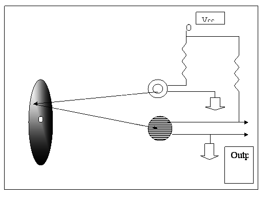
Fig. 1 LED-LDR sensor in reflection mode
Light emitted by the LED is directed towards the outer core of the wheel. The outer core has one white mark against a black background. When the black background is exposed to incident light the reflected energy is low and the resistor value of LDR remains unaffected. As the white portion of the core faces incident radiation, it reflects most of the energy. This reflected light falls on the LDR causing the resistance to drop. Voltage across the output also drops. If there is only one white spot on the wheel the RPM shall be,
60 * frequency of sensor output
The resolution and speed of measurement can be increased to desired level by having multiple black & white stripes.
Another possible arrangement is to use a toothed wheel and place the LED-LDR combination in such away that the teeth interrupt the passage of light between LED and LDR.
THE 8751 MICROCONTROLLER
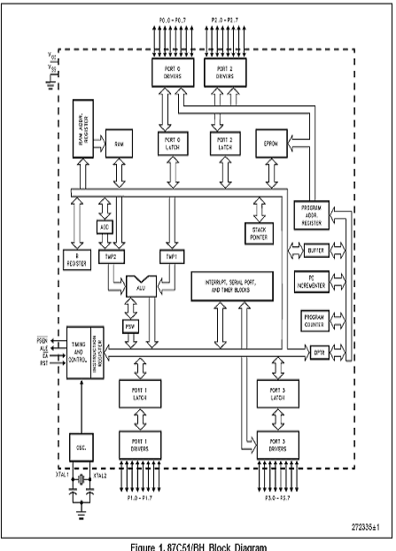
The 8051 is an 8 bit microcontroller originally developed by Intel in 1980. It is the world's most popular microcontroller core, made by many independent manufacturers (truly multi-sourced).
An 8751 contains:
- CPU with Boolean processor
- 5 interrupts of which 2 are external 2 priority levels
- 2 * 16-bit timer/ counters
- Programmable full-duplex serial port
(Baud rate provided by one of the timers)
- 32 I/O lines (four 8-bit ports)
- RAM
- 4Kbyte EPROM in some models
The
8751 instruction set is optimized for the one-bit operations so often
desired in real-world, real-time control applications. The Boolean processor
provides direct support for bit manipulation. This leads to more efficient
programs that need to deal with binary input and output conditions inherent
in digital-control problems. Bit addressing can be used for test pin
monitoring or program control flags.
SPECIFICATIONS OF 87C51
CHMOS SINGLE-CHIP 8-BIT MICROCONTROLLER
Commercial/ Express 87C51
■ High Performance CHMOS EPROM
■ 12 MHz Operation
■ Improved Quick-Pulse Programming Algorithm
■ 3-Level Program Memory Lock
■ Boolean Processor
■ 128-Byte Data RAM
■ 32 Programmable I/O Lines
■ Two 16-Bit Timer/Counters
■ Extended Temperature Range (-40°C to +85°C)
■ 5 Interrupt Sources
■ Programmable Serial Port
■ TTL- and CMOS-Compatible Logic Levels
■ 64K External Program Memory Space
■ 64K External Data Memory Space
MEMORY ORGANIZATION:
Program memory: Up to 4 Kbytes of the program memory can reside on-chip. In addition the device can address up to 64K of program memory external to the chip.
Data memory: This microcontroller has a 128 x 8 on-chip RAM. In addition it can address up to 64 Kbytes of external data memory.
The Intel 87C51 is a single-chip control-oriented Microcontroller which is fabricated on Intel's reliable CHMOS III-E technology. Being a member of the MCS® 51 controller family, the 87C51 uses the same powerful instruction set, has the same architecture, and is pin-for-pin compatible with the existing MCS 51 controller family of products.
PIN OUT DETAILS
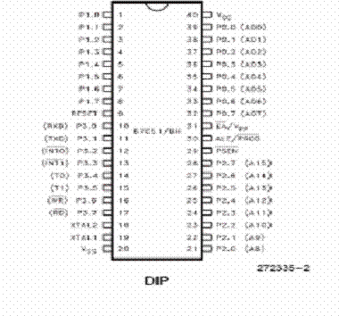
PIN DESCRIPTION:
VCC: Supply voltage.
VSS: Circuit ground.
Port 0: Port 0 is an 8-bit open drain bidirectional I/O port. As an output port each pin can sink several LS TTL inputs. Port 0 pins that have 1's written to them float, and in that state can be used as high-impedance inputs. Port 0 is also the multiplexed low-order address and data bus during accesses to external memory. In this application it uses strong internal pull-ups when emitting 1's.
Port 0 also receives the code bytes during EPROM programming, and outputs the code bytes during program verification. External pull-ups are required during program verification.
Port 1: Port 1 is an 8-bit bidirectional I/O port with internal pull-ups. The Port 1 output buffers can drive LS TTL inputs. Port 1 pins that have 1's written to them are pulled high by the internal pull-ups, and in that state can be used as inputs. As inputs, Port 1pins that are externally pulled low will source current (IIL, on the data sheet) because of the internal pull-ups.
Port 1 also receives the low-order address bytes during EPROM programming and program verification.
Port 2: Port 2 is an 8-bit bidirectional I/O port with internal pull-ups. Port 2 pins that have 1's written to them are pulled high by the internal pull-ups, and in that state can be used as inputs. As inputs, Port 2 pins that are externally pulled low will source current (IIL, on the data sheet) because of the internal pull-ups.
Port 2 emits the high-order address byte during fetches from external Program memory and during accesses to external Data Memory that use 16-bit address (MOVX @DPTR). In this application it uses strong internal pull-ups when emitting 1's. During accesses to external Data Memory that use 8-bit addresses (MOVX @Ri), Port 2 emits the contents of the P2 Special Function Register.
Port 2 also receives some control signals and the high-order address bits during EPROM programming and program verification.
Port 3: Port 3 is an 8-bit bidirectional I/O port with internal pull-ups. The Port 3 output buffers can drive LS TTL inputs. Port 3 pins that have 1's written to them are pulled high by the internal pull-ups, and in that state can be used as inputs. As inputs, Port 3 pins that are externally pulled low will source current (IIL, on the data sheet) because of the pull-ups.
Port 3 also serves the functions of various special features of the MCS-51 Family, as listed below:
Pin Name Alternate Function
P3.0 RXD Serial input line
P3.1 TXD Serial output line
P3.2 INT0 External Interrupt 0
P3.3 INT1 External Interrupt 1
P3.4 T0 Timer 0 external input
P3.5 T1 Timer 1 external input
P3.6 WR External Data Memory Write strobe
P3.7 RD External Data Memory Read strobe
Port 3 also receives some control signals for EPROM programming and program verification.
RST: Reset input. A high on this pin for two machine cycles while the oscillator is running resets the device. The port pins will be driven to their reset condition when a minimum VIH1 voltage is applied whether the oscillator is running or not. An internal pull down resistor permits a power-on reset with only a capacitor connected to VCC.
ALE/PROG: Address Latch Enable output signal for latching the low byte of the address during accesses to external memory. This pin is also the program pulse input (PROG) during EPROM programming for the 87C51. If desired, ALE operation can be disabled by setting bit 0 of SFR location 8EH. With this bit set, the pin is weakly pulled high. However, the ALE disable feature will be suspended during a MOVX or MOVC instruction, idle mode, power down mode and ICE mode. The ALE disable feature will be terminated by reset. When the ALE disable feature is suspended or terminated, the ALE pin will no longer be pulled up weakly. Setting the ALE-disable bit has no effect if the microcontroller is in external execution mode. In normal operation ALE is emitted at a constant rate of 1/6 the oscillator frequency, and may be used for external timing or clocking purposes. Note, however, that one ALE pulse is skipped during each access to external Data Memory.
PSEN: Program Store Enable is the Read strobe to External Program Memory. When the 87C51/BH is executing from Internal Program Memory, PSEN is inactive (high). When the device is executing code from External Program memory, PSEN is activated twice each machine cycle, except that two PSEN activations are skipped during each access to external Data Memory.
EA/V PP: External Access enable. EA must be strapped to VSS in order to enable the 87C51/BH to fetch code from External Program Memory locations starting at 0000H up to FFFFH. Note, however, that if either of the Lock Bits is programmed, the logic level at EA is internally latched during reset. EA must be strapped to VCC for internal program execution. This pin also receives the programming supply voltage (VPP) during EPROM programming.
XTAL1: Input to the inverting oscillator amplifier.
XTAL2: Output from the inverting oscillator amplifier.
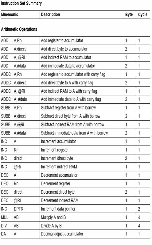
INSTRUCTION SET:
The instruction set is divided in to 5 categories. They are as follows:
1. Arithmetic instructions.
2. Logic instructions.
3. Data transfer instructions.
4. Boolean variable manipulation instruction.
5. Program and machine control instruction.


CIRCUIT DIAGRAMS

Circuit Diagram for signal conditioning circuit

PROGRAM CODING
****** LISTING of (XYZ) ******
LINE LOC OBJECT SOURCE
1 0000 ;******************************************************
2 0000 B: EQU 0F0H ; B REGISTER
3 0000 ACC: EQU 0E0H ; ACCUMULATOR
4 0000 PSW: EQU 0D0H ; PROGRAM
STATUS WORD
5 0000 IEC: EQU 0A8H ; INTERRUPT
ENABLE
6 0000 P1: EQU 90H ; PORT 1
7 0000 P2: EQU 0A0H ; PORT 2
8 0000 TH1: EQU 8DH ; TIMER 1 HIGH
9 0000 TH0: EQU 8CH ; TIMER 0 HIGH
10 0000 TL1: EQU 8BH ; TIMER 1 LOW
11 0000 TL0: EQU 8AH ; TIMER 0 LOW
12 0000 TMOD: EQU 89H ; TIMER MODE
13 0000 TCON: EQU 88H ; TIMER
CONTROL
14 0000 DPH: EQU 83H ; DATA POINTER
HIGH
15 0000 DPL: EQU 82H ; DATA POINTER
LOW
16 0000 SP: EQU 81H ; STACK
POINTER
17 0000 ;---------MCS-51 INTERNAL BIT ADDRESSES
18 0000 CY: EQU 0D7H ; CARRY FLAG
19 0000 RS1: EQU 0D4H ; REGISTER
SELECT MSB
20 0000 RS0: EQU 0D3H ; REGISTER
SELECT LSB
21 0000 EA: EQU 0AFH ; ENABLE ALL
INTERUPPT
22 0000 ET1: EQU 0ABH ; ENABLE TIMER
1 INTERUPPT
23 0000 EX1: EQU 0AAH ; ENABLE
EXTERNAL 1
INTERR
24 0000 ET0: EQU 0A9H ; ENABLE TIMER
0 INTERUPPT
25 0000 EX0: EQU 0A8H ; ENABLE
EXTERNAL 0
INTERR
26 0000 TF1: EQU 08FH ; TIMER 1
OVERFLOW
FLAG
27 0000 TR1: EQU 08EH ; TIMER 1 RUN
CONTROL BIT
28 0000 TF0: EQU 08DH ; TIMER 0
OVERFLOW
FLAG
29 0000 TR0: EQU 08CH ; TIMER 0 RUN
CONTROL BIT
30 0000 IE1: EQU 08BH ; EXT INTERR. 1
EDGE FLAG
31 0000 IT1: EQU 08AH ; EXT INTERR. 1
TYPE FLAG
32 0000 IE0: EQU 089H ; EXT INTERR. 0
EDGE FLAG
33 0000 IT0: EQU 088H ; EXT INTERR. 0
TYPE FLAG
34 0000
35 0000 ; ---------DEVICE ADDRESS TABLE HERE
36 0000
37 0000 ; ---------RAM ADDRESS HERE
38 0000 PINF: EQU 030H ; PARA
ENTRY
FLAG 1
39 0000 NUM: EQU 031H ; NO. TO
DECIDE THE
LOWER LT.
40 0000 BEEP: EQU 033H ; BEEPER
FLAG 1
41 0000 DEG1: EQU 034H ; DIGITS
TEMP
STORAGE 8
42 0000 TEMP: EQU 038H ; TEMPORARY
STORAGE 4
43 0000 COUNT EQU 03CH ; TO SAVE THE
VALUE OF COUNT
44 0000 OP1: EQU 03EH ; OPERAND 1
FOR MATHS LINK 4
45 0000 OP2: EQU 043H ; OPERAND 2
FOR MATHS LINK 4
46 0000
47 0000 ; -------END OF address DECLARATIONS
48 0000
49 0000
50 0000 ORG 0000H ; MAIN BODY PROGRAM
51 0000 01 30 [2] AJMP MAIN
52 0002 ORG001BH ; JUMP FOR
TIMER 1
53 001B 02 01 41 [2] LJMP TINT ; INTERUPPT
HANDLER
54 001E
55 001E ORG 0030H
56 0030 75 81 60 [2] MAIN: MOVSP, #060H ; LOAD STACK
POINTER
57 0033 74 00 [1] MOV A, #00H ; CLEARS THE
COUNTER = 0
58 0035 F5 8C [1] MOV TH0, A
59 0037 F5 8A [1] MOV TL0, A
60 0039 C2 D7 [1] CLR CY
61 003B 90 03 E8 [2] MOV DPTR, #1000
62 003E 74 FF [1] MOV A, #0FFH
63 0040 95 82 [1] SUBB A, DPL
64 0042 F5 31 [1] MOV NUM, A
65 0044 74 FF [1] MOV A, #0FFH
66 0046 95 83 [1] SUBB A, DPH
67 0048 F5 32 [1] MOV NUM+1, A
68 004A 75 89 15 [2] MOV TMOD, #15H ; SELECTING
THE MODE
OF 0PERATION
69 004D 85 32 8D [2] MOV TH1, NUM+1
; SPECIFYING
THE LIMITS
70 0050 85 31 8B [2] MOV TL1, NUM ; ---"---
71 0053 D2 8E [1] SETB TCON.6 ; STARTS
TIMER
72 0055 D2 8C [1] SETB TCON.4 ; STARTS
COUNTER
73 0057 D2 AB [1] SETB ET1 ; TIMER
INT. ENABLED
74 0059 D2 AF [1] SETB EA ; ENABLE
INT. OF TIMER
75 005B ; -- CODE FOR MAIN-LOOP, RESIDES HERE
76 005B E5 3C [1] CODE: MOV A, COUNT
77 005D F5 38 [1] MOV TEMP, A ; COPYING TO
TEMP ARRAY
78 005F E5 3D [1] MOV A, COUNT+1
79 0061 F5 39 [1] MOV TEMP+1, A
80 0063 ;****************
81 0063 11 91 [2] ACALL BINBCD ; WE WILL GET
ASCII VALUE
IN DEG1-4
82 0065 ;***************
83 0065 C2 D7 [1] CLR CY ; LOOP TO
CONVERT THE
NO. INTO HEX
84 0067 AB 04 [2] MOV R3, 04
85 0069 78 34 [1] MOV R0, #DEG1
86 006B E6 [1] LOOP1: MOV A,@R0
87 006C 54 0F [1] ANL A, #0FH
88 006E F6 [1] MOV @R0, A
89 006F 08 [1] INC R0
90 0070 DB F9 [2] DJNZ R3, LOOP1
91 0072 ;**************
92 0072 E5 34 [1] MOV A, DEG1
93 0074 C4 [1] SWAP A
94 0075 45 35 [1] ORL A, DEG1+1 ; FORMING THE
COMPLETE NO.
95 0077 F5 A0 [1] MOV P2, A ; 23 FROM 02
AND 03
96 0079 ; AND SENDING
IT TO PORT 1 & 2
97 0079 E5 36 [1] MOV A, DEG1+2
98 007B C4 [1] SWAP A
99 007C 45 37 [1] ORL A, DEG1+3
100 007E F5 90 [1] MOV P1, A
101 0080
102 0080 01 5B [2] AJMP CODE ; MOVES TO
THE STARTING OF
THE CODE
103 0082
104 0082 ; ----------------------------------------------------------
105 0082 79 20 [1] DELAY: MOV R1, #020H
106 0084 78 01 [1] MOV R0, #01H
107 0086 D8 FE [2] DLY2: DJNZ R0, DLY2
108 0088 D9 FC [2] DJNZ R1, DLY2
109 008A 22 [2] RET
110 008B ; ----------------------------------------------------------
111 008B 74 00 [1] RSET0: MOV A,#00H
112 008D FC [1] MOV R4, A
113 008E FD [1] MOV R5, A
114 008F FE [1] MOV R6, A
115 0090 22 [2] RET
116 0091 ; ROUTINE TO CONVERT 24 BIT BINARY
NO. TO 7 DIGIT ASCII
117 0091 75 3A 00 [2] BINBCD: MOV TEMP+2, #00H
; LOAD 0 TEMP+2
118 0094 11 8B [2] ACALL RSET0 ; R4, 5, 6 =0
119 0096 85 38 3E [2] MOV OP1, TEMP
120 0099 85 39 3F [2] MOV OP1+1, TEMP+1
121 009C 85 3A 40 [2] MOV OP1+2, TEMP+2
122 009F 75 3A 0A [2] MOV DEG1+6, #0AH
; 0ADEG1= -VE SIGN
123 00A2 31 25 [2] ACALL SB3
124 00A4 31 3A [2] ACALL MTR4
125 00A6 7B 2F [1] BCDCOV: MOV R3, #02FH
; COUNT= -1,FF
126 00A8 31 33 [2] ACALL MR4T
127 00AA 75 3E A0 [2] MOV OP1, #0A0H ;10^5
128 00AD 75 3F 86 [2] MOV OP1+1, #086H
129 00B0 75 40 01 [2] MOV OP1+2, #01H
130 00B3 0B [1] LPL: INC R3
131 00B4 31 25 [2] ACALL SB3
132 00B6 40 04 [2] JC LPLX
133 00B8 31 3A [2] ACALL MTR4
134 00BA 80 F7 [2] SJMP LPL
135 00BC 8B 39 [2] LPLX: MOV DEG1+5, R3
; STORE
136 00BE 7B 2F [1] MOV R3, #02FH ; COUNT=-1FF
137 00C0 31 33 [2] ACALL MR4T
138 00C2 75 3E 10 [2] MOV OP1, #010H ; 10^4
139 00C5 75 3F 27 [2] MOV OP1+1, #027H
140 00C8 75 40 00 [2] MOV OP1+2, #0
141 00CB 0B [1] LPTH: INC R3
142 00CC 31 25 [2] ACALL SB3
143 00CE 40 04 [2] JC LPTHX
144 00D0 31 3A [2] ACALL MTR4
145 00D2 80 F7 [2] SJMP LPTH
146 00D4 8B 38 [2] LPTHX: MOV DEG1+4, R3
; STORE
147 00D6 7B 2F [1] MOV R3, #02FH
; COUNT=-1 FF
148 00D8 31 33 [2] ACALL MR4T
149 00DA 75 3E E8 [2] MOV OP1, #0E8H ; 10^3
150 00DD 75 3F 03 [2] MOV OP1+1, #03H
151 00E0 75 40 00 [2] MOV OP1+2,#0
152 00E3 0B [1] LPHO: INC R3
153 00E4 31 25 [2] ACALL SB3
154 00E6 40 04 [2] JC LPHOX
155 00E8 31 3A [2] ACALL MTR4
156 00EA 80 F7 [2] SJMP LPHO
157 00EC 8B 37 [2] LPHOX: MOV DEG1+3, R3
; STORE
158 00EE 7B 2F [1] MOV R3, #02FH ; COUNT=-1FF
159 00F0 31 33 [2] ACALL MR4T
160 00F2 75 3E 64 [2] MOV OP1, #064H ; 10^2
161 00F5 75 3F 00 [2] MOV OP1+1, #0
162 00F8 75 40 00 [2] MOV OP1+2, #0
163 00FB 0B [1] LPH: INC R3
164 00FC 31 25 [2] ACALL SB3
165 00FE 40 04 [2] JC LPHX
166 0100 31 3A [2] ACALL MTR4
167 0102 80 F7 [2] SJMP LPH
168 0104 8B 36 [2] LPHX: MOV DEG1+2, R3
; STORE
169 0106 7B 2F [1] MOV R3, #02FH ; COUNT=-1 FF
170 0108 31 33 [2] ACALL MR4T
171 010A 75 3E 0A [2] MOV OP1, #0AH ; 10^1
172 010D 75 3F 00 [2] MOV OP1+1, #0
173 0110 75 40 00 [2] MOV OP1+2, #0
174 0113 0B [1] LPT: INC R3
175 0114 31 25 [2] ACALL SB3
176 0116 40 04 [2] JC LPTX
177 0118 31 3A [2] ACALL MTR4
178 011A 80 F7 [2] SJMP LPT
179 011C 8B 35 [2] LPTX: MOV DEG1+1, R3
; STORE
180 011E E5 38 [1] MOV A, TEMP
181 0120 24 30 [1] ADD A, #30H
182 0122 F5 34 [1] MOV DEG1, A
183 0124 22 [2] RET
184 0125 C3 [1] SB3: CLR C
185 0126 EC [1] MOV A, R4 ; SUBTRACT
LSB
186 0127 95 3E [1] SUBB A, OP1
187 0129 FC [1] MOV R4, A
188 012A ED [1] MOV A, R5
189 012B 95 3F [1] SUBB A, OP1+1
190 012D FD [1] MOV R5, A
191 012E EE [1] MOV A, R6
192 012F 95 40 [1] SUBB A, OP1+2
193 0131 FE [1] MOV R6, A
194 0132 22 [2] RET
195 0133 AC 38 [2] MR4T: MOV R4, TEMP
196 0135 AD 39 [2] MOV R5, TEMP+1
197 0137 AE 3A [2] MOV R6, TEMP+2
198 0139 22 [2] RET
199 013A 8C 38 [2] MTR4: MOV TEMP, R4
200 013C 8D 39 [2] MOV TEMP+1, R5
201 013E 8E 3A [2] MOV TEMP+2, R6
202 0140 22 [2] RET
203 0141
204 0141 ; -------------------------------
205 0141 C0 E0 [2] TINT: PUSH ACC ; SAVE ACC
206 0143 C0 D0 [2] PUSH PSW ; SAVE PSW
207 0145 C0 82 [2] PUSH DPL ; SAVE DPTR
208 0147 C0 83 [2] PUSH DPH ; **ALL SAVING'S DONE**
209 0149 D2 D4 [1] SETB RS1 ; SELECT
REGISTER
BANK 1
210 014B C2 D3 [1] CLR RS0 ; REGISTER
BANK CHANGED
211 014D E5 8C [1] MOV A, TH0 ; SAVING THE
COUNTER
VALUE
212 014F F5 3D [1] MOV COUNT+1, A
213 0151 E5 8A [1] MOV A, TL0
214 0153 F5 3C [1] MOV COUNT, A
215 0155 74 00 [1] MOV A, #00H ; CLEARS THE
COUNTER = 0
216 0157 F5 8C [1] MOV TH0, A
217 0159 F5 8A [1] MOV TL0, A
218 015B C2 D7 [1] CLR CY
219 015D 75 89 15 [2] MOV TMOD, #15H ; SELECTING
THE MODE OF
OPERATION
220 0160 85 32 8D [2] MOV TH1, NUM+1 ; SPECIFING
THE LIMITS
221 0163 85 31 8B [2] MOV TL1, NUM ; ---"---
222 0166 D2 8E [1] SETB TCON.6 ; START TIME
223 0168 D2 8C [1] SETB TCON.4 ; STARTS
COUNTER
224 016A D2 AB [1] SETB ET1 ; TIMER INT.
ENABLED
225 016C D2 AF [1] SETB EA ; ENABLE INT
OF TIMER
226 016E D0 83 [2] NMCOP: POP DPH ; INTERUPPT
RETURN
SEQUENCE
227 0170 D0 82 [2] POP DPL
228 0172 D0 D0 [2] POP PSW
229 0174 D0 E0 [2] POP ACC
230 0176 32 [2] RETI
231 0177 END
********** SYMBOLTABLE (62 symbols) **********
B :00F0 ACC :00E0 PSW :00D0 IEC :00A8
P1 :0090 P2 :00A0 TH1 :008D TH0 :008C
TL1 :008B TL0 :008A TMOD :0089 TCON :0088
DPH :0083 DPL :0082 SP :0081 CY :00D7
RS1 :00D4 RS0 :00D3 EA :00AF ET1 :00AB
EX1 :00AA ET0 :00A9 EX0 :00A8 TF1 :008F
TR1 :008E TF0 :008D TR0 :008C IE1 :008B
IT1 :008A IE0 :0089 IT0 :0088 PINF :0030
NUM :0031 BEEP :0033 DEG1 :0034 TEMP :0038
COUNT :003C OP1 :003E OP2 :0043 MAIN :0030
CODE :005B LOOP1 :006B DELAY :0082 DLY2 :0086
RSET0 :008B BINBCD :0091 BCDCOV :00A6 LPL :00B3
LPLX :00BC LPTH :00CB LPTHX :00D4 LPHO :00E3
LPHOX :00EC LPH :00FB LPHX :0104 LPT :0113
LPTX: 011C SB3 :0125 MR4T :0133 MTR4 :013A
TINT :0141 NMCOP :016E
CONCLUSION
An optical pair consisting of a Light Emitting Diode (LED infrared) and a Light Dependent Resistor (LDR) configured in reflection mode with fly wheel pained in alternating black and white sectors on in transmission mode with the fly wheel having saw-tooth indentations on periphery, yields pulse waveform at its output across the LDR. The frequency of the output is proportional to the RPM. The sensor can be used for measurement of RPM and number of revolutions integration. Using this circuit we can thus measure RPM of any rotating structure such as motor etc. Whenever the wheel rotates the light from LED is reflected from a sector. More light shall get reflected from white sectors whereas black sectors shall reflect less light. LDR correspondingly shall depict less and more resistance. The output across the LDR shall be pulses in cohesion with the alternating sectors of the wheel. These pulses are then converted into digital form using an amplifier and comparator circuit to make them TTL compatible.
This digital output has been given to the microprocessor 8751. Timer 1 input pin was connected to this input with and the timer was used in event counter mode. Timer 0 was used to limit the time of measurement. Counts registered within the interval of timer 0 were used as measurement. The counts were displayed on the seven segment LED displays. The displays were driven through BCD to seven segment decoder chip74247. The seven segment decoder chip drives the seven segment display and generates the pattern desired by BCD input.
The BCD input of 74247 were driven by port 1 and port 2 outputs of the microprocessor. Each port has 8 pins. A BCD output requires 4 lines. Two decoders and correspondingly two displays are driven by a single port. The use of two ports thus allows four BCD numbers being displayed on the LEDs.
As frequency is directly proportional to the RPM which is readable on LED display.
The entire circuit was assembled and tested. It is possible to build a small processing system using 8751 whenever the number of inputs is restricted and are in digital form. The Boolean processing feature of 8751 provides very powerful tool for digital control application.
Contribute content or training
reports / feedback / Comments
Practical
Training reports
All rights reserved © copyright
123ENG